|
|
|
|||
|
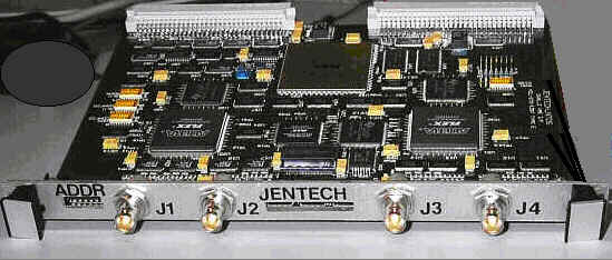
The TI TMS320LC549 DSP used on the Dual E board is designed specifically for embedded communications applications and is a familiar sight in many modems and cell phones. The DSP is particularly well suited to this NTDS application due to its high speed robust I/O, zero local wait state internal RAM, deterministic cache and Harvard based computer architecture. The three DSP processors used on the Dual E board provide 200 MIPS of processing power and are allocated as follows: DSP 1 supports processing for NTDS Interface 1 DSP 2 supports processing for NTDS Interface 2 DSP 3 supports non-NTDS processing In addition to operational programs, the DSP internal memory allows for on-chip storage of data such as NTDS buffering, ALU accumulators and index registers, currently executing instructions, chain house keeping tables and VME interrupt queuing. (See the topic "The Benefits of Using DSPs" for more information about the DSP processors.) An Altera 600 pin FPGA/BGA performs the task of high speed VMEbus controller and is supported by a set of address and data transceivers. VME I/O requests are queued internal to the FPGA and are FIFOed on and off the board independent of the other processors. Therefore, NTDS processing continues in parallel with VMEbus I/O and an FPGA-to-DSP interrupt is generated upon completion. This distribution of processing power eliminates the standard method of sequential processing used on most NTDS interface products and allows an allocation of tasks resulting in true parallel processing. The Dual E board design incorporates technology advances that have occurred since many of the older NTDS products were designed. The use of low voltage (3.3v) and ultra-low voltage (2.5v) components allows the Dual E board to be clocked at much higher rates, producing the high performance needed to support two interfaces while still maintaining low power consumption, low noise and minimal heat dissipation and cooling requirements. The hardware components and board layout used were specifically selected to increase product reliability and ease of manufacture. The combination of a single PCB with non-socketed surface mount components minimizes the profile of the Dual E board and makes the board more rugged and less susceptible to contaminants, oxidation, humidity, vibration and damage from handling. All active components are mounted on a single side, allowing for better test point access as well as a simplified assembly process. The component manufacturers selected have an excellent history of product line support including clear paths to next generation products negating obsolescence concerns. See the "RAM and FLASH Memories" highlight for a discussion of on-board memory resources. See the "High Resolution NTDS Transmit and Receive" highlight for a discussion of the analog hardware circuitry. See the "The Benefits of Using DSPs" highlight for a discussion of the DSP devices used and high speed parallel processing architecture. See the "High Performance VMEbus Interface" highlight for a discussion of the Altera 600 pin BGA and the high speed VMEbus controller.
|